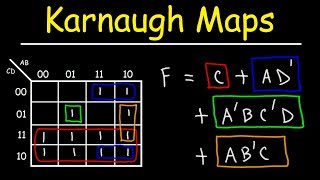
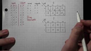
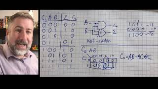
Media Summary: We take a look at the fundamentals of how computers work. We start with a look at This video tutorial provides an introduction into karnaugh maps and In this video I go over how to do a timing diagram for a simple

07 1 Logic Design Combinational - Detailed Analysis & Overview

We take a look at the fundamentals of how computers work. We start with a look at This video tutorial provides an introduction into karnaugh maps and In this video I go over how to do a timing diagram for a simple This electronics video provides a basic introduction into This video series starts at the very beginning and shows each step in the

Photo Gallery

Digital Logic Fundamentals: Combinational Circuits
Digital logic #7: Combinational logic including the encoder, decoder, and multiplexer
Understanding Logic Gates
Introduction to Karnaugh Maps - Combinational Logic Circuits, Functions, & Truth Tables
Basic Timing Diagrams for Combinational Logic Circuits
Logic Gates, Truth Tables, Boolean Algebra   AND, OR, NOT, NAND & NOR
HOW TO: Combinational logic: Truth Table → Karnaugh Map → Minimal Form → Gate Diagram
Design a combinational circuit with three inputs, x , y , and z , and three outputs, A, B , and C .
1) Designing Combinational Logic Circuit
Combinational Devices 1: Half Adder and Full Adder
View Detailed Profile
Digital Logic Fundamentals: Combinational Circuits

Digital Logic Fundamentals: Combinational Circuits

An overview of

Digital logic #7: Combinational logic including the encoder, decoder, and multiplexer

Digital logic #7: Combinational logic including the encoder, decoder, and multiplexer

Summary: This lecture extends

Understanding Logic Gates

Understanding Logic Gates

We take a look at the fundamentals of how computers work. We start with a look at

Introduction to Karnaugh Maps - Combinational Logic Circuits, Functions, & Truth Tables

Introduction to Karnaugh Maps - Combinational Logic Circuits, Functions, & Truth Tables

This video tutorial provides an introduction into karnaugh maps and

Basic Timing Diagrams for Combinational Logic Circuits

Basic Timing Diagrams for Combinational Logic Circuits

In this video I go over how to do a timing diagram for a simple

Logic Gates, Truth Tables, Boolean Algebra   AND, OR, NOT, NAND & NOR

Logic Gates, Truth Tables, Boolean Algebra AND, OR, NOT, NAND & NOR

This electronics video provides a basic introduction into

HOW TO: Combinational logic: Truth Table → Karnaugh Map → Minimal Form → Gate Diagram

HOW TO: Combinational logic: Truth Table → Karnaugh Map → Minimal Form → Gate Diagram

https://learnfrom.stevenpetryk.com/

Design a combinational circuit with three inputs, x , y , and z , and three outputs, A, B , and C .

Design a combinational circuit with three inputs, x , y , and z , and three outputs, A, B , and C .

Design

1) Designing Combinational Logic Circuit

1) Designing Combinational Logic Circuit

Chapter 3:

Combinational Devices 1: Half Adder and Full Adder

Combinational Devices 1: Half Adder and Full Adder

This video series starts at the very beginning and shows each step in the