Media Summary: Grab your free Design Mistakes Checklist Bundle: ... Hey Everyone, Hope you all are doing well ! This side Satyamraj Sinha technical Creater at Electronics Globe. In this i have ... NOTE 1: I should have mentioned in the video that you can force recalculation of these polygons using the "B" key (or whatever ...
Basic Kicad 2 Layer Pcb - Detailed Analysis & Overview
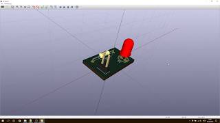
Grab your free Design Mistakes Checklist Bundle: ... Hey Everyone, Hope you all are doing well ! This side Satyamraj Sinha technical Creater at Electronics Globe. In this i have ... NOTE 1: I should have mentioned in the video that you can force recalculation of these polygons using the "B" key (or whatever ... 21 How to move the component between top and bottom The full Workshop* : _ In this video of the Zero to Maker ...