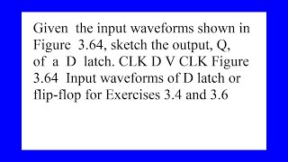
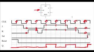
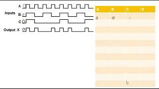
Media Summary: The logic circuit shown has the input waveforms ‘A’ and ‘B’ as shown. Pick out the correct output waveform :- Input A Input B ... Hello. In this lesson you will learn about the Please like this video if you found it helpful.

Given The Input Waveforms Shown - Detailed Analysis & Overview

The logic circuit shown has the input waveforms ‘A’ and ‘B’ as shown. Pick out the correct output waveform :- Input A Input B ... Hello. In this lesson you will learn about the Please like this video if you found it helpful. This video is on basic logic gate timing diagram. AND logic gate output timing diagram is drawn when both the This video is on basic logic gate timing diagram. OR gate followed by AND logic gate output timing diagram is drawn when all the ... ... do one more timing diagram this is very similar to the last one except this schematic shows that this is an active low

The logic circuit shown below has the input waveforms ‘A’ and ‘B’ as shown. Pick out the correct output waveform. (Input ... In this video, we determine the output of a NAND Gate for the This video tells how to design digital logic circuit when

Photo Gallery

The logic circuit shown has the input waveforms ‘A’ and ‘B’ as shown. Pick out the correct output
Waveforms of Basic Logic Gates | Digital Logic Design | Digital Electronics | Undergrad Academy
Given the input waveforms shown in Figure 3.64 sketch the output Q of a D latch CLK Figure 3.64 I...
Basic Timing Diagrams
Basic logic gate timing diagram/ waveform of basic logic gate/digital electronics
Output waveform of basic logic gate / digital logic design
The Fig shown input waveforms A and B to a logic gate. Draw the output waveform for an
JK Flip Flop Timing Diagrams
The logic circuit shown has the input waveforms 'A' and 'B' as shown. Pick out the correct
The logic circuit shown below has the input waveforms ‘A’ and ‘B’ as shown. Pick out the correct
NAND Gate Output from Input Waveform | Logic Gates Timing Diagram Explained 12
Digital Logic Circuit Design by Given input and Output waveform/ Digital Logic
View Detailed Profile
The logic circuit shown has the input waveforms ‘A’ and ‘B’ as shown. Pick out the correct output

The logic circuit shown has the input waveforms ‘A’ and ‘B’ as shown. Pick out the correct output

The logic circuit shown has the input waveforms ‘A’ and ‘B’ as shown. Pick out the correct output waveform :- Input A Input B ...

Waveforms of Basic Logic Gates | Digital Logic Design | Digital Electronics | Undergrad Academy

Waveforms of Basic Logic Gates | Digital Logic Design | Digital Electronics | Undergrad Academy

Hello. In this lesson you will learn about the

Given the input waveforms shown in Figure 3.64 sketch the output Q of a D latch CLK Figure 3.64 I...

Given the input waveforms shown in Figure 3.64 sketch the output Q of a D latch CLK Figure 3.64 I...

Given the input waveforms shown

Basic Timing Diagrams

Basic Timing Diagrams

Please like this video if you found it helpful.

Basic logic gate timing diagram/ waveform of basic logic gate/digital electronics

Basic logic gate timing diagram/ waveform of basic logic gate/digital electronics

This video is on basic logic gate timing diagram. AND logic gate output timing diagram is drawn when both the

Output waveform of basic logic gate / digital logic design

Output waveform of basic logic gate / digital logic design

This video is on basic logic gate timing diagram. OR gate followed by AND logic gate output timing diagram is drawn when all the ...

The Fig shown input waveforms A and B to a logic gate. Draw the output waveform for an

The Fig shown input waveforms A and B to a logic gate. Draw the output waveform for an

The Fig

JK Flip Flop Timing Diagrams

JK Flip Flop Timing Diagrams

... do one more timing diagram this is very similar to the last one except this schematic shows that this is an active low

The logic circuit shown has the input waveforms 'A' and 'B' as shown. Pick out the correct

The logic circuit shown has the input waveforms 'A' and 'B' as shown. Pick out the correct

Please add description.The logic circuit

The logic circuit shown below has the input waveforms ‘A’ and ‘B’ as shown. Pick out the correct

The logic circuit shown below has the input waveforms ‘A’ and ‘B’ as shown. Pick out the correct

The logic circuit shown below has the input waveforms ‘A’ and ‘B’ as shown. Pick out the correct output waveform. (Input ...

NAND Gate Output from Input Waveform | Logic Gates Timing Diagram Explained 12

NAND Gate Output from Input Waveform | Logic Gates Timing Diagram Explained 12

In this video, we determine the output of a NAND Gate for the

Digital Logic Circuit Design by Given input and Output waveform/ Digital Logic

Digital Logic Circuit Design by Given input and Output waveform/ Digital Logic

This video tells how to design digital logic circuit when

The logic circuit shown below has the input waveforms ‘A’ and ‘B’ as shown. Pick out the correct out

The logic circuit shown below has the input waveforms ‘A’ and ‘B’ as shown. Pick out the correct out

Q 7. The logic circuit