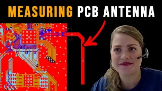
Media Summary: Multidisciplinary product creation powered by your unconstrained network. Work concurrently across I come up with this a long time ago and keep using it all the time. Links: - To learn If you have a PCB antenna on your board, you need to know this. Thank you very much Kaja Sørbotten from Nordic ...

How To Design Rf Trace - Detailed Analysis & Overview

Multidisciplinary product creation powered by your unconstrained network. Work concurrently across I come up with this a long time ago and keep using it all the time. Links: - To learn If you have a PCB antenna on your board, you need to know this. Thank you very much Kaja Sørbotten from Nordic ... AD: This video includes a paid promotion for JLCPCB.) Some tips for when What's the difference between a transmission line and a

Photo Gallery

How to Design RF Trace Tapers (With Free Calculator!)
Flawless PCB design: RF rules of thumb - Part 1
Altium Rapid Tutorial - RF Impedance Matching
Useful TIP: What Track Width To Use When Routing PCB?
Why Your Ground Design is WRONG — and How to Fix It. Flawless PCB design part 6
PCB Antenna - How To Design, Measure And Tune
Simple Universal RF Amplifier PCB Design - From Schematic to Measurements
RF Design in the PCB: Transmission lines (coplanar)
(Sponsored) Practical RF Hardware and PCB Design Tips - Phil's Lab #19
Michael Ossmann: Simple RF Circuit Design
PCB Traces 101 - Phil's Lab #112
RF Design in the PCB: Edge Plating
View Detailed Profile
How to Design RF Trace Tapers (With Free Calculator!)

How to Design RF Trace Tapers (With Free Calculator!)

Multidisciplinary product creation powered by your unconstrained network. Work concurrently across

Flawless PCB design: RF rules of thumb - Part 1

Flawless PCB design: RF rules of thumb - Part 1

Full course info: https://www.hans-rosenberg.com/epdc_information_yt?utm_source=yt-d-v1 Free mini-course: ...

Altium Rapid Tutorial - RF Impedance Matching

Altium Rapid Tutorial - RF Impedance Matching

How to impedance match an

Useful TIP: What Track Width To Use When Routing PCB?

Useful TIP: What Track Width To Use When Routing PCB?

I come up with this a long time ago and keep using it all the time. Links: - To learn

Why Your Ground Design is WRONG — and How to Fix It. Flawless PCB design part 6

Why Your Ground Design is WRONG — and How to Fix It. Flawless PCB design part 6

Full course info: https://www.hans-rosenberg.com/epdc_information_yt?utm_source=yt-d-v6 Free mini-course: ...

PCB Antenna - How To Design, Measure And Tune

PCB Antenna - How To Design, Measure And Tune

If you have a PCB antenna on your board, you need to know this. Thank you very much Kaja Sørbotten from Nordic ...

Simple Universal RF Amplifier PCB Design - From Schematic to Measurements

Simple Universal RF Amplifier PCB Design - From Schematic to Measurements

Full course info: https://www.hans-rosenberg.com/epdc_information_yt?utm_source=yt-d-v7 Free mini-course: ...

RF Design in the PCB: Transmission lines (coplanar)

RF Design in the PCB: Transmission lines (coplanar)

Multidisciplinary product creation powered by your unconstrained network. Work concurrently across

(Sponsored) Practical RF Hardware and PCB Design Tips - Phil's Lab #19

(Sponsored) Practical RF Hardware and PCB Design Tips - Phil's Lab #19

AD: This video includes a paid promotion for JLCPCB.) Some tips for when

Michael Ossmann: Simple RF Circuit Design

Michael Ossmann: Simple RF Circuit Design

This workshop on Simple

PCB Traces 101 - Phil's Lab #112

PCB Traces 101 - Phil's Lab #112

Basics and guidelines for PCB

RF Design in the PCB: Edge Plating

RF Design in the PCB: Edge Plating

Multidisciplinary product creation powered by your unconstrained network. Work concurrently across

When Does a Trace Act Like a Transmission Line?

When Does a Trace Act Like a Transmission Line?

What's the difference between a transmission line and a