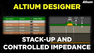
Media Summary: Multidisciplinary product creation powered by your unconstrained network. Work concurrently across design, sourcing, and ... About This Video Learn how to design a 6-layer In this video segment John Coonrod discusses the many variables involved with

Pcb Stackups Impedance Control - Detailed Analysis & Overview

Multidisciplinary product creation powered by your unconstrained network. Work concurrently across design, sourcing, and ... About This Video Learn how to design a 6-layer In this video segment John Coonrod discusses the many variables involved with We all know how important it is to hit target

Photo Gallery

PCB Stack-up and Controlled Impedance in Altium Designer
Standard Stackup + Controlled Impedance Deep Dive
PCB Stack-Up and Build-Up - Phil's Lab #56
GSSG Stackup Deep Dive: Routing, Impedance, and HDI
KiCad Controlled Impedance Traces (e.g. 50Ω) - Phil's Lab #3
Understanding Layer Stackup and Impedance Control in OrCAD X
How to Design a 6-Layer PCB Stackup for Best Performance  #jlcpcb #pcbdesign #stackup
PCB Stackups & Impedance Control
What is Impedance?  - PCB Design and Signal Integrity
Cadence OrCAD PCB Design How to Set Trace Impedance (Signal Integrity)
Controlled Impedance Routing - Altium Academy
What Should Be Considered For Optimal High Frequency Impedance Control?
View Detailed Profile
PCB Stack-up and Controlled Impedance in Altium Designer

PCB Stack-up and Controlled Impedance in Altium Designer

Multidisciplinary product creation powered by your unconstrained network. Work concurrently across design, sourcing, and ...

Standard Stackup + Controlled Impedance Deep Dive

Standard Stackup + Controlled Impedance Deep Dive

Multidisciplinary product creation powered by your unconstrained network. Work concurrently across design, sourcing, and ...

PCB Stack-Up and Build-Up - Phil's Lab #56

PCB Stack-Up and Build-Up - Phil's Lab #56

What a

GSSG Stackup Deep Dive: Routing, Impedance, and HDI

GSSG Stackup Deep Dive: Routing, Impedance, and HDI

Altium Develop unites your

KiCad Controlled Impedance Traces (e.g. 50Ω) - Phil's Lab #3

KiCad Controlled Impedance Traces (e.g. 50Ω) - Phil's Lab #3

How to calculate track widths and layout

Understanding Layer Stackup and Impedance Control in OrCAD X

Understanding Layer Stackup and Impedance Control in OrCAD X

Learn the essentials of layer

How to Design a 6-Layer PCB Stackup for Best Performance  #jlcpcb #pcbdesign #stackup

How to Design a 6-Layer PCB Stackup for Best Performance #jlcpcb #pcbdesign #stackup

About This Video Learn how to design a 6-layer

PCB Stackups & Impedance Control

PCB Stackups & Impedance Control

Learn about material

What is Impedance?  - PCB Design and Signal Integrity

What is Impedance? - PCB Design and Signal Integrity

Become a Professional

Cadence OrCAD PCB Design How to Set Trace Impedance (Signal Integrity)

Cadence OrCAD PCB Design How to Set Trace Impedance (Signal Integrity)

NEW Methodical Method to Hardware &

Controlled Impedance Routing - Altium Academy

Controlled Impedance Routing - Altium Academy

Multidisciplinary product creation powered by your unconstrained network. Work concurrently across design, sourcing, and ...

What Should Be Considered For Optimal High Frequency Impedance Control?

What Should Be Considered For Optimal High Frequency Impedance Control?

In this video segment John Coonrod discusses the many variables involved with

Tips for PCB Stackup Design

Tips for PCB Stackup Design

We all know how important it is to hit target