Media Summary: Multidisciplinary product creation powered by your unconstrained network. Work concurrently across design, sourcing, and ... Rapidly locate the perfect component in all of your libraries with advanced search and parameter Grab your free Design Mistakes Checklist Bundle: ...

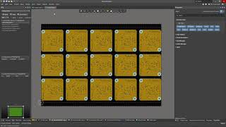
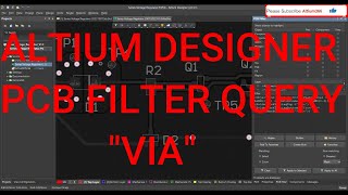
The Pcb Filter Panel Making - Detailed Analysis & Overview

Multidisciplinary product creation powered by your unconstrained network. Work concurrently across design, sourcing, and ... Rapidly locate the perfect component in all of your libraries with advanced search and parameter Grab your free Design Mistakes Checklist Bundle: ... “Want to be job-ready in electronics design? Try Altium Student Lab! You get free access to Altium Designer and Altium 365 ...

Photo Gallery

The PCB Filter Panel | Making Precise Selections in Altium Designer
Altium Designer Tutorial 33: Filtering PCB Design Objects using the PCB Filter Query for "Track".
Altium Designer Layout| Designator: Using PCB filter & Designator Formation
How to do Panelization in Altium Designer
Flawless PCB design: 3 simple rules - Part 2
Making Enclosure Panels Using PCBs - Phil's Lab #102
Altium Designer Tutorial 34:  PCB Filter Query for "VIA".
Altium Designer's Secret PCB Filtering Trick You MUST Know!
Components Panel with Parametric Filters
Altium Designer Tutorial 36: PCB Filter Query to find a "NPTH" that is incorrectly checked as Plated
6 Horribly Common PCB Design Mistakes
Altium Designer Tutorial 35: PCB Filter Query for "Tented and Untented VIA".
View Detailed Profile
The PCB Filter Panel | Making Precise Selections in Altium Designer

The PCB Filter Panel | Making Precise Selections in Altium Designer

Multidisciplinary product creation powered by your unconstrained network. Work concurrently across design, sourcing, and ...

Altium Designer Tutorial 33: Filtering PCB Design Objects using the PCB Filter Query for "Track".

Altium Designer Tutorial 33: Filtering PCB Design Objects using the PCB Filter Query for "Track".

The PCB Filter panel

Altium Designer Layout| Designator: Using PCB filter & Designator Formation

Altium Designer Layout| Designator: Using PCB filter & Designator Formation

How to Do It? Open

How to do Panelization in Altium Designer

How to do Panelization in Altium Designer

Multidisciplinary product creation powered by your unconstrained network. Work concurrently across design, sourcing, and ...

Flawless PCB design: 3 simple rules - Part 2

Flawless PCB design: 3 simple rules - Part 2

Full course info: https://www.hans-rosenberg.com/epdc_information_yt?utm_source=yt-d-v2 Free mini-course: ...

Making Enclosure Panels Using PCBs - Phil's Lab #102

Making Enclosure Panels Using PCBs - Phil's Lab #102

How to design

Altium Designer Tutorial 34:  PCB Filter Query for "VIA".

Altium Designer Tutorial 34: PCB Filter Query for "VIA".

PCB Filter

Altium Designer's Secret PCB Filtering Trick You MUST Know!

Altium Designer's Secret PCB Filtering Trick You MUST Know!

In this video, I introduce the powerful

Components Panel with Parametric Filters

Components Panel with Parametric Filters

Rapidly locate the perfect component in all of your libraries with advanced search and parameter

Altium Designer Tutorial 36: PCB Filter Query to find a "NPTH" that is incorrectly checked as Plated

Altium Designer Tutorial 36: PCB Filter Query to find a "NPTH" that is incorrectly checked as Plated

When

6 Horribly Common PCB Design Mistakes

6 Horribly Common PCB Design Mistakes

Grab your free Design Mistakes Checklist Bundle: ...

Altium Designer Tutorial 35: PCB Filter Query for "Tented and Untented VIA".

Altium Designer Tutorial 35: PCB Filter Query for "Tented and Untented VIA".

The PCB Filter panel

PCB Panelization in Altium Designer | Step-by-Step Tutorial | EP 09 | PCB Design Tutorials #altium

PCB Panelization in Altium Designer | Step-by-Step Tutorial | EP 09 | PCB Design Tutorials #altium

“Want to be job-ready in electronics design? Try Altium Student Lab! You get free access to Altium Designer and Altium 365 ...